


exhibition


Technology News
- Author:
- Source: PCBBUY
- Date: 2021-12-23
- Views: 4448Times
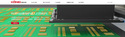
Castellated Hole, also known as plated half-hole is a kind of rampart-like structure designed at the edge of a PCB. They are manufactured by creating ordinary plated holes and then running a sharp router bit across them, leaving half the hole in place.
As a convenient and efficient sideways conduction design, it’s often appears in signal circuits and widely used for board-on-board connections. It is possible to directly weld the edge of the holes with the main board to save connectors and space. For example, the Bluetooth or Wi-Fi module with plated half holes, as an individual part, can be easily soldered to a main board for a specific demand without any wire connection, which is neat and easy to operate.
If you are curious about castellated hole in PCB, please check and read the content below in this passage for more professional knowledge.
Wanna know PCB knowledge? Check and read for more.

1. What are castellated hole used for?
Castellated holes can be used for a couple of different reasons. Most commonly, they are used by designers to create PCB modules, such as Wi-Fi or Bluetooth modules, which will then be used as an independent part to be placed onto another board during the PCB assembly process. However, castellations are also used when combining two boards to ensure the solder inspection joint is properly structured and to create wireless PCB to PCB links.
2. What are the specifications of castellated holes?
Compliance with design attributes
When designing a castellated hole, compliance is necessary. Manufacturers need to comply with all the design attributes. That way, they’ll be able to manufacture boards that meet market expectations. If they happen to skip some steps, then the problem awaits them. Compliance is imperative. If there are steps, you need to follow them. Is there any necessary equipment to use? Don’t ignore them. Compliance is a significant specification when designing castellated holes. It’s as simple as that.
Size
Besides compliance with design attributes, size also matters. According to industry standards, it’s advisable to use the largest sizes. Do you have a chance to use the largest possible size? If so, then use it. But why does size matter? The size of the feature allows the use of any surface finish.
Surface finish
A surface finish is necessary for the design of a castellated hole. When designing castellated holes, surface finishing is essential. Manufacturers use surface finishes for two fundamental reasons: to ensure perfect solderability and protect the exposed copper. Of importance to note is that the surface finish that you use varies. Mostly, it depends on the intended use of your boards. The most recommended finis is ENIG. There are several types of finishes besides ENIG. Others include HASL and OSP, to mention but a few.
Pad Design
Pad design is another design attribute that you need to follow. It is advisable to use the most massive possible pad. It should be both on top and on the bottom of the place. By going for the largest possible residence, rest assured the best-castellated holes. Large pads give you room to drill holes with a lot of ease and precision. For the best results, consider using the most considerable places.
3. How to manufacture castellated holes PCB?
Once you’ve placed the castellated holes onto your PCB, how do you get the bare board fabricated? The goal here is to ensure high quality and yield in a standard process, but castellated holes do not seem to fit into the standard PCB fabrication process. Your fabricator can help you ensure your design will pass through fabrication by modifying the Gerbers to indicate drill hits and required plating along the board edge. This normally requires the following Gerbers (X2 format):
4. Why we process castellated holes PCB?
We use castellated holes PCB for various purposes. Frequently, designers use them to produce printed circuit board modules. Models of these PCB modules include Bluetooth and WIFI modules. We also use serrated holes when connecting two boards. The serrated holes enable excellent wireless connections between circuit boards.
We use serrated holes for various reasons
Mostly, designers use them to create PCB modules. Examples of these PCB modules include Bluetooth and WiFi modules. We also use serrated holes when connecting two boards. The serrated holes enable excellent wireless connections between circuit boards.
Easily change the pin layout of components
The keyhole is proper when redesigning the pin. These castellated holes allow the designer to change the design of the pen easily. Sometimes, users may have different layout requirements for their contacts. With serrated holes, it is relatively easy to change the position of the pin.
Verify solder joint quality
Designers use castellated holes to combine two boards. Regarding the quality of solder joints, crimp holes play an important role. They are helpful as they help in validating the quality of the solder joint.
As a convenient and efficient sideways conduction design, it’s often appears in signal circuits and widely used for board-on-board connections. It is possible to directly weld the edge of the holes with the main board to save connectors and space. For example, the Bluetooth or Wi-Fi module with plated half holes, as an individual part, can be easily soldered to a main board for a specific demand without any wire connection, which is neat and easy to operate.
If you are curious about castellated hole in PCB, please check and read the content below in this passage for more professional knowledge.
Wanna know PCB knowledge? Check and read for more.
1. What are castellated hole used for?
Castellated holes can be used for a couple of different reasons. Most commonly, they are used by designers to create PCB modules, such as Wi-Fi or Bluetooth modules, which will then be used as an independent part to be placed onto another board during the PCB assembly process. However, castellations are also used when combining two boards to ensure the solder inspection joint is properly structured and to create wireless PCB to PCB links.
2. What are the specifications of castellated holes?
Compliance with design attributes
When designing a castellated hole, compliance is necessary. Manufacturers need to comply with all the design attributes. That way, they’ll be able to manufacture boards that meet market expectations. If they happen to skip some steps, then the problem awaits them. Compliance is imperative. If there are steps, you need to follow them. Is there any necessary equipment to use? Don’t ignore them. Compliance is a significant specification when designing castellated holes. It’s as simple as that.
Size
Besides compliance with design attributes, size also matters. According to industry standards, it’s advisable to use the largest sizes. Do you have a chance to use the largest possible size? If so, then use it. But why does size matter? The size of the feature allows the use of any surface finish.
Surface finish
A surface finish is necessary for the design of a castellated hole. When designing castellated holes, surface finishing is essential. Manufacturers use surface finishes for two fundamental reasons: to ensure perfect solderability and protect the exposed copper. Of importance to note is that the surface finish that you use varies. Mostly, it depends on the intended use of your boards. The most recommended finis is ENIG. There are several types of finishes besides ENIG. Others include HASL and OSP, to mention but a few.
Pad Design
Pad design is another design attribute that you need to follow. It is advisable to use the most massive possible pad. It should be both on top and on the bottom of the place. By going for the largest possible residence, rest assured the best-castellated holes. Large pads give you room to drill holes with a lot of ease and precision. For the best results, consider using the most considerable places.
3. How to manufacture castellated holes PCB?
Once you’ve placed the castellated holes onto your PCB, how do you get the bare board fabricated? The goal here is to ensure high quality and yield in a standard process, but castellated holes do not seem to fit into the standard PCB fabrication process. Your fabricator can help you ensure your design will pass through fabrication by modifying the Gerbers to indicate drill hits and required plating along the board edge. This normally requires the following Gerbers (X2 format):
- Copper layers (GTL and GBL)
- Solder mask openings defined on both board surfaces (GTS and GBS)
- Drill files (TXT/DRL)
4. Why we process castellated holes PCB?
We use castellated holes PCB for various purposes. Frequently, designers use them to produce printed circuit board modules. Models of these PCB modules include Bluetooth and WIFI modules. We also use serrated holes when connecting two boards. The serrated holes enable excellent wireless connections between circuit boards.
We use serrated holes for various reasons
Mostly, designers use them to create PCB modules. Examples of these PCB modules include Bluetooth and WiFi modules. We also use serrated holes when connecting two boards. The serrated holes enable excellent wireless connections between circuit boards.
Easily change the pin layout of components
The keyhole is proper when redesigning the pin. These castellated holes allow the designer to change the design of the pen easily. Sometimes, users may have different layout requirements for their contacts. With serrated holes, it is relatively easy to change the position of the pin.
Verify solder joint quality
Designers use castellated holes to combine two boards. Regarding the quality of solder joints, crimp holes play an important role. They are helpful as they help in validating the quality of the solder joint.
Previous: SMT process inspection of PCB assembly
Next: PCBA包装外包的优势
Friendship link


版权所有 ©深圳市亚中咨询有限公司
电话:0755-25856945 邮箱:pzl88smt@126.com 网址:www.smt668.com
地址:深圳市罗湖区怡正发大厦 SMT专业网版权所有(c) 2010 粤ICP备17073069号
本站部分图文来源网络,如有侵权问题请通知我们处理!
做网站维护